Home > Press > Stanford engineers perfecting carbon nanotubes for highly energy-efficient computing
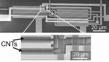 |
| An electron microscope image showing carbon nanotube transistors (CNTs) arranged in an integrated logic circuit. Photo: Stanford University School of Engineering |
Abstract:
Carbon nanotubes represent a significant departure from traditional silicon technologies and offer a promising path to solving the challenge of energy efficiency in computer circuits, but they aren't without challenges. Now, engineers at Stanford have found ways around the challenges to produce the first full-wafer digital logic structures based on carbon nanotubes.
Energy efficiency is the most significant challenge standing in the way of continued miniaturization of electronic systems, and miniaturization is the principal driver of the semiconductor industry. "As we approach the ultimate limits of Moore's Law, however, silicon will have to be replaced in order to miniaturize further," said Jeffrey Bokor, deputy director for science at the Molecular Foundry at the Lawrence Berkeley National Laboratory and Professor at UC-Berkeley.
To this end, carbon nanotubes (CNTs) are a significant departure from traditional silicon technologies and a very promising path to solving the challenge of energy efficiency. CNTs are cylindrical nanostructures of carbon with exceptional electrical, thermal and mechanical properties. Nanotube circuits could provide a ten-times improvement in energy efficiency over silicon.
Early promise
When the first rudimentary nanotube transistors were demonstrated in 1998, researchers imagined a new age of highly efficient, advanced computing electronics. That promise, however, is yet to be realized due to substantial material imperfections inherent to nanotubes that left engineers wondering whether CNTs would ever prove viable.
Over the last few years, a team of Stanford engineering professors, doctoral students, undergraduates, and high-school interns, led by Professors Subhasish Mitra and H.-S. Philip Wong, took on the challenge and has produced a series of breakthroughs that represent the most advanced computing and storage elements yet created using CNTs.
These high-quality, robust nanotube circuits are immune to the stubborn and crippling material flaws that have stumped researchers for over a decade, a difficult hurdle that has prevented the wider adoption of nanotube circuits in industry. The advance represents a major milestone toward Very-large Scale Integrated (VLSI) systems based on nanotubes.
"The first CNTs wowed the research community with their exceptional electrical, thermal and mechanical properties over a decade ago, but this recent work at Stanford has provided the first glimpse of their viability to complement silicon CMOS transistors," said Larry Pileggi, Tanoto Professor of Electrical and Computer Engineering at Carnegie Mellon University and director of the Focus Center Research Program Center for Circuit and System Solutions.
Major barriers
While there have been significant accomplishments in CNT circuits over the years, they have come mostly at the single-nanotube level. At least two major barriers remain before CNTs can be harnessed into technologies of practical impact: First, "perfect" alignment of nanotubes has proved all but impossible to achieve, introducing detrimental stray conducting paths and faulty functionality into the circuits; second, the presence of metallic CNTs (as opposed to more desirable semiconducting CNTs) in the circuits leads to short circuits, excessive power leakage and susceptibility to noise. No CNT synthesis technique has yet produced exclusively semiconducting nanotubes.
"Carbon nanotube transistors are attractive for many reasons as a basis for dense, energy efficient integrated circuits in the future. But, being borne out of chemistry, they come with unique challenges as we try to adapt them into microelectronics for the first time. Chief among them is variability in their placement and their electrical properties. The Stanford work, that looks at designing circuits taking into consideration such variability, is therefore an extremely important step in the right direction," Supratik Guha, Director of the Physical Sciences Department at the IBM Thomas J. Watson Research Center .
"This is very interesting and creative work. While there are many difficult challenges ahead, the work of Wong and Mitra makes good progress at solving some of these challenges," added Bokor.
Realizing that better processes alone will never overcome these imperfections, the Stanford engineers managed to circumvent the barriers using a unique imperfection-immune design paradigm to produce the first-ever full-wafer-scale digital logic structures that are unaffected by misaligned and mis-positioned CNTs. Additionally, they addressed the challenges of metallic CNTs with the invention of a technique to remove these undesirable elements from their circuits.
Striking features
The Stanford design approach has two striking features in that it sacrifices virtually none of CNTs' energy efficiency and it is also compatible with existing fabrication methods and infrastructure, pushing the technology a significant step toward commercialization.
"This transformative research is made all the more promising by the fact that it can co-exist with today's mainstream silicon technologies, and leverage today's manufacturing and system design infrastructure, providing the critical feature of economic viability," said Betsy Weitzman of the Focus Center Research Program at the Semiconductor Research Corporation
The engineers next demonstrated the possibilities of their techniques by creating the essential components of digital integrated systems: arithmetic circuits and sequential storage, as well as the first monolithic three-dimensional integrated circuits with extreme levels of integration.
The Stanford team's work was featured recently as an invited paper at the prestigious International Electron Devices Meeting (IEDM) as well as a "keynote paper" in the prestigious IEEE Transactions on Computer-Aided Design of Integrated Circuits and Systems.
"Many researchers assumed that the way to live with imperfections in CNT manufacturing was through expensive fault-tolerance techniques. Through clever insights, Mitra and Wong have shown otherwise. Their inexpensive and practical methods can significantly improve CNT circuit robustness, and go a long way toward making CNT circuits viable," said Sachin S. Sapatnekar, Editor-in-Chief, IEEE Transactions on CAD. "I anticipate high reader interest in the paper," Sapatnekar noted.
Andrew Myers is associate director for communications for the Stanford University School of Engineering.
Editor's Note: This article first appeared as a "Behind the Scenes" feature on LiveScience in partnership with the National Science Foundation. The researchers depicted in Behind the Scenes have been supported by the National Science Foundation, the federal agency charged with funding basic research and education across all fields of science and engineering. Any opinions, findings, and conclusions or recommendations expressed in this material are those of the author and do not necessarily reflect the views of the National Science Foundation.
####
For more information, please click here
Contacts:
Andrew Myers
Associate Director of Communications
650.736.2245
Jamie Beckett
Director of Communications and Alumni Relations
650.736.2241
Copyright ? Stanford School of Engineering
If you have a comment, please Contact us.Issuers of news releases, not 7th Wave, Inc. or Nanotechnology Now, are solely responsible for the accuracy of the content.
Bookmark:


News and information
![]() Synthesizing Binary Metal Oxide Nanotubes June 14th, 2012
Synthesizing Binary Metal Oxide Nanotubes June 14th, 2012
![]() Painkiller by Photosynthesis June 14th, 2012
Painkiller by Photosynthesis June 14th, 2012
![]() Gone fishing: Researchers' imaging technique trolls in quiet cellular seas June 14th, 2012
Gone fishing: Researchers' imaging technique trolls in quiet cellular seas June 14th, 2012
![]() Switchable nano magnets: Research group at Kiel University switches magnetism of individual molecules June 14th, 2012
Switchable nano magnets: Research group at Kiel University switches magnetism of individual molecules June 14th, 2012
Govt.-Legislation/Regulation/Funding/Policy
![]() Self-assembling nanocubes for next generation antennas and lenses June 13th, 2012
Self-assembling nanocubes for next generation antennas and lenses June 13th, 2012
![]() Looking At and Into the Ultra-Small June 13th, 2012
Looking At and Into the Ultra-Small June 13th, 2012
![]() UCSB Scientists Synthesize First Genetically Evolved Semiconductor Material June 13th, 2012
UCSB Scientists Synthesize First Genetically Evolved Semiconductor Material June 13th, 2012
![]() Ancient effect harnessed to produce electricity from waste heat June 13th, 2012
Ancient effect harnessed to produce electricity from waste heat June 13th, 2012
Chip Technology
![]() UCSB Scientists Synthesize First Genetically Evolved Semiconductor Material June 13th, 2012
UCSB Scientists Synthesize First Genetically Evolved Semiconductor Material June 13th, 2012
![]() U.S. Photovoltaic Manufacturing Consortium Selects Recognized Solar Leaders to Guide the Development of a National CIGS PV Roadmap: Groundbreaking effort to accelerate the deployment of CIGS manufacturing will play a critical role in building a competitive U.S. photovoltaic indus June 13th, 2012
U.S. Photovoltaic Manufacturing Consortium Selects Recognized Solar Leaders to Guide the Development of a National CIGS PV Roadmap: Groundbreaking effort to accelerate the deployment of CIGS manufacturing will play a critical role in building a competitive U.S. photovoltaic indus June 13th, 2012
![]() Dolomite launches new microfluidic interface for quick and reliable PDMS chip connection June 13th, 2012
Dolomite launches new microfluidic interface for quick and reliable PDMS chip connection June 13th, 2012
![]() Tohoku University and imec Partner to Enhance Research and Collaboration Efforts June 11th, 2012
Tohoku University and imec Partner to Enhance Research and Collaboration Efforts June 11th, 2012
Nanotubes/Buckyballs
![]() Synthesizing Binary Metal Oxide Nanotubes June 14th, 2012
Synthesizing Binary Metal Oxide Nanotubes June 14th, 2012
![]() SouthWest NanoTechnologies Announces New Specialty Multi-Wall Carbon Nanotubes for Conductive Polymers June 13th, 2012
SouthWest NanoTechnologies Announces New Specialty Multi-Wall Carbon Nanotubes for Conductive Polymers June 13th, 2012
![]() Software & Solar Power. Prize Money Boosts Research June 12th, 2012
Software & Solar Power. Prize Money Boosts Research June 12th, 2012
![]() ORNL microscopy reveals workings behind promising inexpensive catalyst June 11th, 2012
ORNL microscopy reveals workings behind promising inexpensive catalyst June 11th, 2012
Discoveries
![]() Synthesizing Binary Metal Oxide Nanotubes June 14th, 2012
Synthesizing Binary Metal Oxide Nanotubes June 14th, 2012
![]() Painkiller by Photosynthesis June 14th, 2012
Painkiller by Photosynthesis June 14th, 2012
![]() Gone fishing: Researchers' imaging technique trolls in quiet cellular seas June 14th, 2012
Gone fishing: Researchers' imaging technique trolls in quiet cellular seas June 14th, 2012
![]() Switchable nano magnets: Research group at Kiel University switches magnetism of individual molecules June 14th, 2012
Switchable nano magnets: Research group at Kiel University switches magnetism of individual molecules June 14th, 2012
Announcements
![]() Synthesizing Binary Metal Oxide Nanotubes June 14th, 2012
Synthesizing Binary Metal Oxide Nanotubes June 14th, 2012
![]() Painkiller by Photosynthesis June 14th, 2012
Painkiller by Photosynthesis June 14th, 2012
![]() Gone fishing: Researchers' imaging technique trolls in quiet cellular seas June 14th, 2012
Gone fishing: Researchers' imaging technique trolls in quiet cellular seas June 14th, 2012
![]() Switchable nano magnets: Research group at Kiel University switches magnetism of individual molecules June 14th, 2012
Switchable nano magnets: Research group at Kiel University switches magnetism of individual molecules June 14th, 2012
glen campbell jerusalem artichoke bud shootout aretha franklin stevie wonder new orleans weather new orleans weather
No comments:
Post a Comment
Note: Only a member of this blog may post a comment.